Bending the light with a tiny chip: Silicon chip acts as a lens-free projector, may one day fit in cell phones
Date:
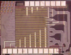
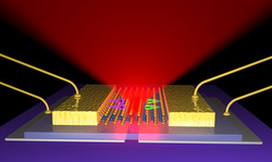
March 11, 2014 Source: California Institute of Technology Summary: Traditional projectors -- like those used to project a film or classroom lecture notes -- pass a beam of light through a tiny image, using lenses to map each point of the small picture to corresponding points on a large screen. A tiny silicon chip eliminates the need for bulky and expensive lenses, and instead projects the image electronically by 'bending the light' with no mechanically moving parts.Imagine that you are in a meeting with coworkers or at a gathering of friends. You pull out your cell phone to show a presentation or a video on YouTube. But you don't use the tiny screen; your phone projects a bright, clear image onto a wall or a big screen. Such a technology may be on its way, thanks to a new light-bending silicon chip developed by researchers at Caltech. The chip was developed by Ali Hajimiri, Thomas G. Myers Professor of Electrical Engineering, and researchers in his laboratory. The results were presented at the Optical Fiber Communication (OFC) conference in San Francisco on March 10. Traditional projectors -- like those used to project a film or classroom lecture notes -- pass a beam of light through a tiny image, using lenses to map each point of the small picture to corresponding, yet expanded, points on a large screen. The Caltech chip eliminates the need for bulky and expensive lenses and bulbs and instead uses a so-called integrated optical phased array (OPA) to project the image electronically with only a single laser diode as light source and no mechanically moving parts. Hajimiri and his colleagues were able to bypass traditional optics by manipulating the coherence of light -- a property that allows the researchers to "bend" the light waves on the surface of the chip without lenses or the use of any mechanical movement. If two waves are coherent in the direction of propagation -- meaning that the peaks and troughs of one wave are exactly aligned with those of the second wave -- the waves combine, resulting in one wave, a beam with twice the amplitude and four times the energy as the initial wave, moving in the direction of the coherent waves. "By changing the relative timing of the waves, you can change the direction of the light beam," says Hajimiri. For example, if 10 people kneeling in line by a swimming pool slap the water at the exact same instant, they will make one big wave that travels directly away from them. But if the 10 separate slaps are staggered -- each person hitting the water a half a second after the last -- there will still be one big, combined wave, but with the wave bending to travel at an angle, he says. Using a series of pipes for the light -- called phase shifters -- the OPA chip similarly slows down or speeds up the timing of the waves, thus controlling the direction of the light beam. To form an image, electronic data from a computer are converted into multiple electrical currents; by applying stronger or weaker currents to the light within the phase shifter, the number of electrons within each light path changes -- which, in turn, changes the timing of the light wave in that path. The timed light waves are then delivered to tiny array elements within a grid on the chip. The light is then projected from each array in the grid, the individual array beams combining coherently in the air to form a single light beam and a spot on the screen. As the electronic signal rapidly steers the beam left, right, up, and down, the light acts as a very fast pen, drawing an image made of light on the projection surface. Because the direction of the light beam is controlled electronically -- not mechanically -- it can create a sort of line very quickly. Since the light draws many times per second, the eye sees the process as a single image instead of a moving light beam, says Hajimiri. "The new thing about our work is really that we can do this on a tiny, one-millimeter-square silicon chip, and the fact that we can do it very rapidly -- rapidly enough to form images, since we phase-shift electronically in two dimensions," says Behrooz Abiri, a graduate student in Hajimiri's group and a coauthor on the paper. So far, the images Hajimiri and his team can project with the current version of the chip are somewhat simple -- a triangle, a smiley face, or single letters, for example. However, the researchers are currently experimenting with larger chips that include more light-delivering array elements that -- like using a larger lens on a camera -- can improve the resolution and increase the complexity of the projected images. In their recent experiments, Hajimiri and his colleagues have used the silicon chip to project images in infrared light, but additional work with different types of semiconductors will also allow the researchers to expand the tiny projector's capabilities into the visible spectrum. "Right now we are using silicon technology, which works better with infrared light. If you want to project visible light, you can take the exact same architecture and do it in what's called compound semiconductor III-V technology," says Firooz Aflatouni, another coauthor on the paper, who in January finished his two-year postdoctoral appointment at Caltech and joined the University of Pennsylvania as an assistant professor. "Silicon is good because it can be easily integrated into electronics, but these other compound semiconductors could be used to do the same thing." "In the future, this can be incorporated into a phone, and since there is no need for a lens, you can have a phone that acts as a projector all by itself," Hajimiri says. However, although the chip could easily be incorporated into a cell phone, he points out that a tiny projection device can have many applications -- including light-based radar systems (called "LIDAR"), which are used in positioning, robotics, geographical measurements, and mapmaking. Such equipment already exists, but current LIDAR technology requires complex, bulky, and expensive equipment -- equipment that could be streamlined and simplified to a single chip at a much lower cost. "But I don't want to limit the device to just a few purposes. The beauty of this thing is that these chips are small and can be made at a very low cost -- and this opens up lots of interesting possibilities," he says. These results were described in a presentation titled "Electronic Two-Dimensional Beam Steering for Integrated Optical Phased Arrays." Along with Hajimiri, Abiri, and Aflatouni, Caltech senior Angad Rekhi also contributed to the work. The study was funded by grants from the Caltech Innovation Initiative, and the Information Science and Technology initiative at Caltech. Story Source: The above story is based on materials provided by California Institute of Technology. The original article was written by Jessica Stoller-Conrad. Note: Materials may be edited for content and length. |
Scientists build thinnest-possible LEDs to be stronger, more energy efficient
Date:
March 10, 2014 Source: University of Washington Summary: Scientists have built the thinnest-known LED that can be used as a source of light energy in electronics. The LED is based off of two-dimensional, flexible semiconductors, making it possible to stack or use in much smaller and more diverse applications than current technology allows.Most modern electronics, from flat-screen TVs and smartphones to wearable technologies and computer monitors, use tiny light-emitting diodes, or LEDs. These LEDs are based off of semiconductors that emit light with the movement of electrons. As devices get smaller and faster, there is more demand for such semiconductors that are tinier, stronger and more energy efficient. University of Washington scientists have built the thinnest-known LED that can be used as a source of light energy in electronics. The LED is based off of two-dimensional, flexible semiconductors, making it possible to stack or use in much smaller and more diverse applications than current technology allows. "We are able to make the thinnest-possible LEDs, only three atoms thick yet mechanically strong. Such thin and foldable LEDs are critical for future portable and integrated electronic devices," said Xiaodong Xu, a UW assistant professor in materials science and engineering and in physics. Xu along with Jason Ross, a UW materials science and engineering graduate student, co-authored a paper about this technology that appeared online March 9 in Nature Nanotechnology. Most consumer electronics use three-dimensional LEDs, but these are 10 to 20 times thicker than the LEDs being developed by the UW. "These are 10,000 times smaller than the thickness of a human hair, yet the light they emit can be seen by standard measurement equipment," Ross said. "This is a huge leap of miniaturization of technology, and because it's a semiconductor, you can do almost everything with it that is possible with existing, three-dimensional silicon technologies," Ross said. The UW's LED is made from flat sheets of the molecular semiconductor known as tungsten diselenide, a member of a group of two-dimensional materials that have been recently identified as the thinnest-known semiconductors. Researchers use regular adhesive tape to extract a single sheet of this material from thick, layered pieces in a method inspired by the 2010 Nobel Prize in Physics awarded to the University of Manchester for isolating one-atom-thick flakes of carbon, called graphene, from a piece of graphite. In addition to light-emitting applications, this technology could open doors for using light as interconnects to run nano-scale computer chips instead of standard devices that operate off the movement of electrons, or electricity. The latter process creates a lot of heat and wastes power, whereas sending light through a chip to achieve the same purpose would be highly efficient. "A promising solution is to replace the electrical interconnect with optical ones, which will maintain the high bandwidth but consume less energy," Xu said. "Our work makes it possible to make highly integrated and energy-efficient devices in areas such as lighting, optical communication and nano lasers." The research team is working on more efficient ways to create these thin LEDs and looking at what happens when two-dimensional materials are stacked in different ways. Additionally, these materials have been shown to react with polarized light in new ways that no other materials can, and researchers also will continue to pursue those applications. Co-authors are Aaron Jones and David Cobden of the UW; Philip Klement of Justus Liebig University in Germany; Nirmal Ghimire, Jiaqiang Yan and D.G. Mandrus of the University of Tennessee and Oak Ridge National Laboratory; Takashi Taniguchi, Kenji Watanabe and Kenji Kitamura of the National Institute for Materials Science in Japan; and Wang Yao of the University of Hong Kong. The research is funded by the U.S. Department of Energy, Office of Science, the Research Grant Council of Hong Kong, the University Grant Committee of Hong Kong and the Croucher Foundation. Ross is supported by a National Science Foundation graduate fellowship. Story Source: The above story is based on materials provided by University of Washington. The original article was written by Michelle Ma. Note: Materials may be edited for content and length. |
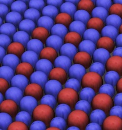
Turing's theory of chemical morphogenesis validated 60 years after his death
Date:
March 10, 2014 Source: Brandeis University Summary: Sixty years after Alan Turing's death, researchers have provided the first experimental evidence that validates Turing's theory of chemical morphogenesis in cell-like structures. This research could impact not only the study of biological development, and how similar patterns form in nature, but materials science as well. Turing's model could help grow soft robots with certain patterns and shapes.Alan Turing's accomplishments in computer science are well known, but lesser known is his impact on biology and chemistry. In his only paper on biology, Turing proposed a theory of morphogenesis, or how identical copies of a single cell differentiate, for example, into an organism with arms and legs, a head and tail. Now, 60 years after Turing's death, researchers from Brandeis University and the University of Pittsburgh have provided the first experimental evidence that validates Turing's theory in cell-like structures. The team published their findings in the Proceedings of the National Academy of Sciences on Monday, March 10. Turing was the first to offer an explanation of morphogenesis through chemistry. He theorized that identical biological cells differentiate, change shape and create patterns through a process called intercellular reaction-diffusion. In this model, a system of chemicals react with each other and diffuse across a space -- say between cells in an embryo. These chemical reactions need an inhibitory agent, to suppress the reaction, and an excitatory agent, to activate the reaction. This chemical reaction, diffused across an embryo, will create patterns of chemically different cells. Turing predicted six different patterns could arise from this model. At Brandeis, Seth Fraden, professor of physics, and Irv Epstein, the Henry F. Fischbach Professor of Chemistry, created rings of synthetic, cell-like structures with activating and inhibiting chemical reactions to test Turing's model. They observed all six patterns plus a seventh unpredicted by Turing. Just as Turing theorized, the once identical structures -- now chemically different -- also began to change in size due to osmosis. This research could impact not only the study of biological development, and how similar patterns form in nature, but materials science as well. Turing's model could help grow soft robots with certain patterns and shapes. More than anything, this research further validates Turing as a pioneer across many different fields, Fraden says. After cracking the German Enigma code, expediting the Allies' victory in World War II, Turing was shamed and ostracized by the British government. He was convicted of homosexuality -- a crime in 1950s England -- and sentenced to chemical castration. He published "The Chemical Basis of Morphogenesis" shortly after his trial and killed himself less than two years later, in June 1954. He was 41 years old. Story Source: The above story is based on materials provided by Brandeis University. Note: Materials may be edited for content and length. |
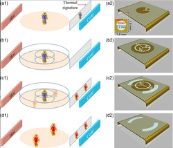
Effective thermal camouflage and invisibility device for soldiers created
Date:
March 11, 2014 Source: National University of Singapore Summary: Scientists have created a thermal illusion device to control thermal camouflage and invisibility using thermotic materials. Every natural object exhibits thermal signatures. However, if these signals are blocked or masked, then these objects become undetectable. The new device can block thermal signatures (leading to invisibility) and provide illusionary camouflage at the same time. This cloaking technology is cost-effective, easily scalable, as well as applicable to even bigger objects (such as soldiers on night missions), and it has also overcome limitations like narrow bandwidth and polarization-dependence. The technology is ready to roll out for military applications.Engineers and scientists have been trying to discover the ultimate "cloaking" device -- not just as a hat trick to make things invisible -- but for its applications in defense technology. Now, a team from the NUS Department of Electrical & Computer Engineering led by Dr Qiu Chengwei, has successfully come out with a thermal illusion device to control thermal camouflage and invisibility using thermotic materials. Thermotics is a branch of science dealing with heat and thermodynamics. Every natural object exhibits thermal signatures. However, if these signals are blocked or masked, then these objects become undetectable. If you can remember the Predator movie (starring Arnold Schwarzenegger) -- the creature is invisible and is also effectively camouflaged to blend in with its surroundings making it difficult for it to be tracked down. But this hi-tech creature has an advantage over its hunters as it detects them using thermal imaging. A "predator" like the one in the movie Predator, to some extent, is actually realizable, using Dr Qiu's invention. His device could block thermal signatures (leading to invisibility) and provide illusionary camouflage at the same time. He and his team's findings were published recently in Advanced Materials as well as Physical Review Letters. Besides academic journals, the researchers' breakthrough has also been extensively highlighted by online scientific publications in the US and UK. Said Dr Qiu, "This is the first time that such a cloak has been proven to work effectively, based on thermotics. Our success means that now we have a cloaking technology that is cost-effective and easily scalable and applicable to even bigger objects such as soldiers on night missions. We have managed to control the thermal illusions' shapes, material properties, distributions, and locations using bulk natural materials without sophisticated fabrication. This drastically overcomes practical and challenging limitations of metamaterials which are not found in nature and hence would require complicated and complex design to imbue them with special properties. Our new technology has also overcome limitations like narrow bandwidth and polarisation-dependence." The team comprising Dr Qiu, Dr Han Tiancheng, Ms Bai Xue, Associate Professor John T L Thong and Professor Li Baowen (NUS Department of Physics), has carefully investigated their device in both time-dependent and temperature-dependent conditions and have found it to demonstrate excellent thermodynamic performance. The technology is ready to roll out for military applications. Their research has also introduced a new dimension to the emerging field of "phononics" which is the controlling and manipulating of heat flow with phonons (particles which transmit heat within solid materials). A spinoff application of their research, said Dr Qiu, would be in heat management of highly packed electronic circuits, interconnectors and batteries. Story Source: The above story is based on materials provided by National University of Singapore. Note: Materials may be edited for content and length. |
